| Status Report of the HADES Drift Chamber Read Out B, G, W | K. Heidel, R. Dressler, O. Fateev1, R. Kotte, L. Naumann | ||
|---|---|---|---|
|
The first module out of six multiwire drift chambers (MDC) designed for plane III of the HADES dielectron spectrometer [1] at GSI Darmstadt has been built and tested successfully [2]. The following report resumes the results of the electronics tests. 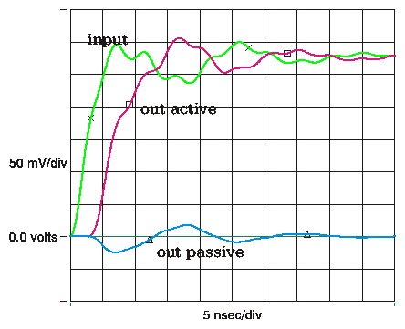
Fig. 1 Crosstalk output active/passive (8%) for a 24 cm long PCB connector and a 27 cm long FPC cable. 1. Simulation: In order to avoid secondary transmission line effects accurate pre-layout simulations, including crosstalk and reflection, have been performed for the printed circuit boards (PCB) developed to guide the signals from the MDC sense wires to the front-end electronics. The layout has been designed as a four-layer PCB with a thick dielectric between signal and ground layers and conductor widths of 0.1 mm to match the input impedance (Z0 = 115 W) of the daughterboards (analog boards with ASD8 chips [3]). The simulation (cf. Fig. 1) yielded typical crosstalks of less than 8% for the common configuration of PCB and flex print cable (FPC [4]), where the latter one connects PCB and daughterboards. The capacity of MDC sense wire, PCB, and FPC, which is important for the input noise characteristics, was measured directly to be about 30 pF, depending on the wire length.
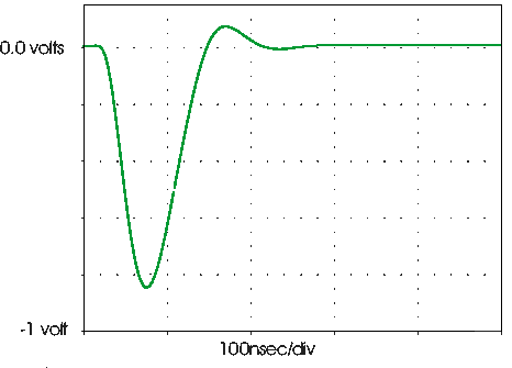
Fig. 2 Simulated output signal for a 10 mA current signal and a detector capacity of 30 pF. 2. Pulse characteristics: A wire chamber acts as a current source with signals depending on the cell geometry, the gas filling and the electric field. A current-sensitive amplifier with a gain of dVout/dIin = 100 mV/mA has been developed [5] to match the small rise time of several ns (according to the collection time of electrons produced near to the sense wire) and the long fall time of about 50 - 100 ns (slow ion drift towards the cathode and field wires). Fig. 2 shows the result of the simulation for a 10 mA current signal. It is in agreement with the amplitude measured at the real amplifier output. 3. Concept of grounding: The front-end electronics consisting of daughterboards (incorporating the ASD8 chips with preamplifier, shaper, and discriminator; thus delivering logical time-above-threshold signals) and motherboards (carrying the TDC's to convert the information) is mounted at the edges of the detector frames. In order to obtain an optimum signal-to-noise ratio special attention has been payed to the grounding principle. The most effective grounding methods with respect to low noise level and small r.f. reception was figured out to be the following: 1) Using short flexible cables with high cross section, all PCB cards and also all analog and digital ground points of the daughterboards have been connected to a broad self-adhesive copper foil glued onto the frame below the motherboards. 2) A thick copper-track loop has been installed around the frame to conduct the reverse current (total 25 A!) back from the daughterboards and motherboards. With this arrangement an unrivaled low noise level of 20 mV (measured at the analog output of a daughterboard) without any disturbing r.f. crosstalk, e.g. arising from the 5 MHz quartz oscillator (clock) operating on the motherboard, has been attained. 1JINR, Dubna, Russia
References
|