High-Energy Ion Implantation
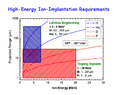 High-energy ion implantation has been well-established in production technology of a number of semiconductor devices. Known advantages of targeted doping, defect creation, or a combination of both are utilized with high-energy ion implantation.
High ion energies of typically some megaelectron-volts (MeV) induce high ion penetration depths in material, thus, facilitating buried doping or defect profiles, unlike any other technology.
Low fluences of 1010 to 1013 cm-2 in typical application fields make the high-energy ion implantation also financially attractive.
Typical application fields of high-energy ion implantation include:
- Implantation of light ions (H, He) to improve the switching behavior in power electronic semiconductor devices (power diodes, thyristors, or power MOSFETs)
- Implantation of doping elements (H, B, P, As, ...) to tune field strength distributions in photodiodes, particle detectors or high-voltage devices
- Implantation of heavy ions to improve emission characteristics of laser diodes
Following implantation chambers and wafer handling systems are offered to perform high-energy ion implantation at our 6 MV Tandetron and 3 MV Tandetron high-energy ion accelerators:
6 MV Tandetron
|
|
High Voltage Engineering Europa B.V. |
|
|
Duoplasmatron model 358 + Li charge exchange channel (only for He-) Cs sputter source, model 860C |
|
|
0.3 - 6 MV |
|
|
0.6 - 50 MeV (depending on charge state) |
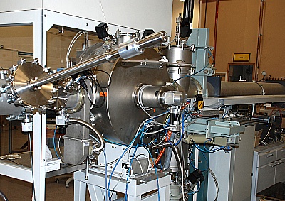
(I) Channel 3: Single wafer implantation chamber
 |
|
|
x, y electrostatic (f ≈ 1 kHz) |
|
|
wafers or other planar samples |
|
|
up to 150 mm wafers |
|
|
7° (other on request) |
|
|
no cooling, typically room temperature |
|
|
starting from 1x1010 cm-2 |
|
|
class 6 (DIN EN ISO 14644) |
|
|
typically 20 per h (depending on fluence) |
|
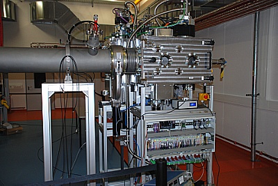
(II) Channel B2: Automated wafer handler
 |
|
|
≤ 150 mm: x, y electrostatic;
>150mm, combination of electrostatic/mechanic |
|
|
wafers only |
|
|
up to 200 mm wafers |
|
|
7° (other on request) |
|
|
no cooling, typically room temperatur |
|
|
starting from 1x1010 cm-2 |
|
|
class 5 (DIN EN ISO 14644) |
|
|
up to 50 per h (depending on fluence) |
|
3 MV Tandetron
|
|
High Voltage Engineering Europa B.V. |
|
|
Duoplasmatron model 358 + Li-charge exchange channel (only for He-) Cs sputter source, model 860C |
|
|
0.1 - 3 MV |
|
|
0.2 - 8 MeV (depending on charge state) |
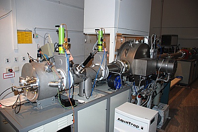
(I) Channel 2: Single wafer, large implantation chamber
 |
|
|
x, y electrostatic (f ≈ 1 kHz) |
|
|
wafers or other planar samples |
|
|
up to 125 mm wafers |
|
|
7° |
|
|
no cooling, typically room temperature |
|
|
starting from 5x1010 cm-2 |
|
|
class 5 (DIN EN ISO 14644) |
|
|
typically 20 per h (depending on fluence) |
|
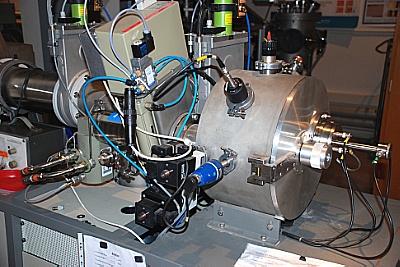
(II) Channel 2: Single wafer, small implantation chamber
 |
|
|
x, y electrostatic (f ≈ 1 kHz) |
|
|
wafers or other planar samples |
|
|
up to 100 mm wafers |
|
|
7° or 0° |
|
|
from LN2 up to 800 °C |
|
|
starting from 5x1010 cm-2 |
|
|
not controlled |
|
|
typically 10 per h (depending on fluence) |
|
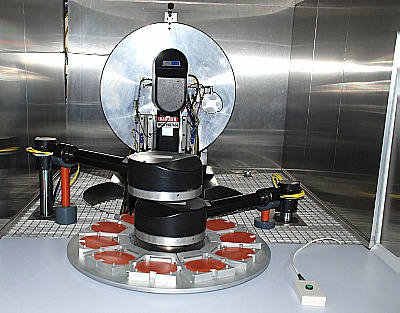
(III) Channel 4: Semi-automated wafer handler EATON NV-10
 |
|
|
x, y (mechanic) |
|
|
wafers only |
|
|
100 mm, 125 mm and 150 mm wafers |
|
|
7° |
|
|
no cooling, typically room temperature |
|
|
starting from 1x1012 cm-2 |
|
|
class 5 (DIN EN ISO 14644) |
|
|
up to 100 per h |
|
High-energy ion implantation has been well-established in production technology of a number of semiconductor devices. Known advantages of targeted doping, defect creation, or a combination of both are utilized with high-energy ion implantation.


