Tantal Based Thin Film Diffusion Barriers
 |
 |
|
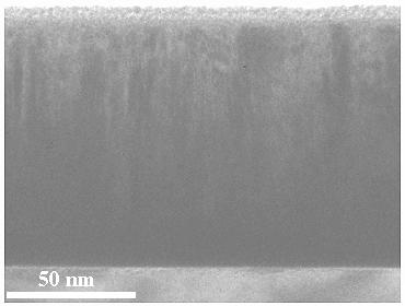
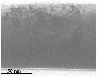
Fig. 1: XTEM images showing the destruction of the columnar structure of an as-deposited 100 nm Ta layer by implantation of 3x10¹⁷ N+/cm2 (65 keV):
(a) as-deposited |
(b) after implantation |
In advanced metallization technology of microelectronic devices the substitution of Al by Cu demands highly effective diffusion barriers. Ta is a very promising material for such barriers. However for barrier thickness below about 50 nm it begins to fail due to defects like grain boundaries and pores.
Ta-based thin film barriers have been treated by ion implantaion of nitrogen and oxygen to decrease the density of diffusion enhancing defects by amorphization or the formation of new phases as nitrides or oxides.
Nitrogen implantation leads to lattice expansion, amorphization and formation of nitrides with increasing dose. For oxygen implantation the dose range is more extended in which amorphization is obtained. Fig.1 shows the destruction of the dangerous columnar microstructure of the sputter deposited Ta layer by nitride formation due to high dose nitrogen implantation.
Ta(Si) layers are amorphous already after sputter deposition. In such systems the thermal stability of the amorphous state is enhanced by implantation of oxygen and nitrogen as shown in Fig.2. The pure Ta(Si) recristallizes already at 650°C while the oxygen implantad film remains still amorphous at this temperature. After nitrogen implantation the amorphous structure is retained also at 800°C.
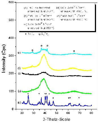 |
Fig.2: XRD pattern of a 100 nm Ta(Si) layer demonstrating enhancement of the thermal stability of the amorphous state: (a) pure Ta(Si) - recrystallized after 650°C/1h, (b) + (c) amorphous until 800°C due to 3x10¹⁷ N+/cm2 (65 keV), (d) + (e) amorphous until 650°C and recrystallized after 800°C/1h due to 3x10¹⁷ O+/cm2 (70 keV), |
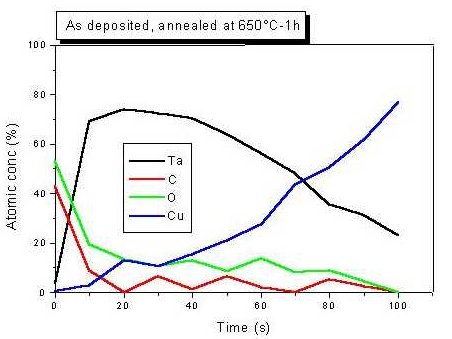
Another approach to improve the barrier effect is ion beam mixing of the interface Ta/Cu.
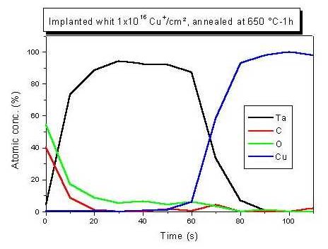
Implantation of 1x10¹⁶ Cu+/cm2 into the interface of a 50 nm Ta film on Cu results in an about 5 nm broad amorphous interlayer. In this way the penetration of Cu into the Ta layer by annealing at 650°C is strongly reduced as shown in Fig.3.
 |
 |
|
(a) AES spectra of the untreated material - penetration of Cu into Ta
|
(b) AES spectra of the ion beam mixed system - no Cu penetration
|
This work is sponsored by the Saxonian Ministry of Science and Arts (SMWK) and carried out in cooperation with TU Dresden, Institut für Halbleiter- und Mikrosystemtechnik and FhG Institut für Zerstörungsfreie Prüfverfahren Dresden (EAQD).

