Department Ion Beam Center
The department Ion Beam Center focuses on the modification and analysis of solid surfaces by the use of ions in a wide energy range (eV to MeV). The department ensures the operation and the methodical development of a variety of ion beam and plasma techniques. The use of facilities for materials research occures in close collaboration with other institute departmentals. In addition to ion beam analysis, for a comprehensive characterization of materials electron microscopy (TEM, SEM, cross-beam systems), and X-ray-based analysis techniques are used for structural elucidation. R&D work using ion-induced effects or structures for opto-and nanoelectronic devices can be performed in a class 100 clean room.
User Access
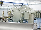
The Ion Beam Center is an internationally leading center of competence for the application of ion beams in materials research. Plasma and ion sources generate ions of all species at energies between eV and 60 MeV.
Head: Dr. Stefan Facsko
Project groups

The ion implanter group provides facilities for the ion-beam induced modification of solid samples in an energy range of 100 eV to 1 MeV. It is possible to irradiate surfaces up to a size of 200 mm in diameter. The ion implantation is used for both basic research and practical investigations in the field of the modification of surface sensitive properties as well as for doping and nanostructering in the semiconductor industry.
Group leader:
Ulrich Kentsch
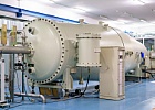
High energy ion beams can be used as fine instruments for analyzing of materials and modifying their electrical, optical, magnetic and other properties in microscopic and macroscopic scales. The main activity of the devision of ion accelerators is operation and development of ion beam systems for material analysis and for material modification as well as scientific and technical support of novel experiments with ion beams (development of new ion optical elements for laser accelerator and new methods of ion implantation, experiments with ion beams for nuclear physics, etc.)
Group leader:
Dr. Shavkat Akhmadaliev
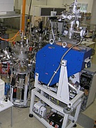
The ion beam analysis group is focused on the non-destructive and quantitative elemental analysis of surfaces and interfaces with ion beams. Various state-of-the-art ion beam analysis techniques are applied that allow highest depth resolution (nm), smallest structures (50nm) and lowest detection limits (ppm). In unique multi-purpose experimental chambers, these techniques are partially combined with complementary structural analysis and sample preparation techniques.
Group leader:
Dr. René Heller
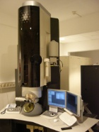
The group Structure Analysis deals with the analysis of the structural, morphological, and chemical properties of nanostructured materials, in particular of (ion-modified) solid surfaces and thin film systems. For this purpose, analytical techniques using the interaction of electrons and X-ray beams with the nanomaterials are applied.
Group leader:
Dr. René Hübner
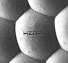
The ion induced nanostructure research group studies processes during the interaction of low energy (10 eV – 50 keV) ions of various charge states with materials. The focus lies on the controlled modification and nano-patterning of surfaces. Such modifications can be material removal through sputtering of surface atoms but also near surface ion beam mixing, ion beam induced defect engineering, or implantation of guest atoms. To achieve this goal we employ low energy broad beam irradiation, highly charged ion beams (HCI), focused liquid metal alloy ion beams (LMAIS FIB) as well as helium ion microscopy (HIM).
Group leader:
Dr. G. Hlawacek
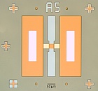
The main goal of our work at the Institute of Ion Beam Physics and Materials Research is the development of novel (opto-)electronic devices based on modification and structuring of both cutting-edge and traditional materials. Through ion beam irradiation facilities at the Ion Beam Center (IBC) various optical/electronic and physical properties of almost any material can be precisely controlled. Final integration into electronic circuits for device testing is achieved by processing in a class 100 (ISO 5) cleanroom using standard semiconductor industry processes and is suitable to pattern sub-µm devices. Electron beam lithography process are run in close collaboration with the nanostructure group at the IBC, where devices as small as 10 nm can be fabricated. Materials currently under investigation range from organic molecules (e.g. conducting Polymers), 2-dimensional semiconductors (e.g. MoS2 and black phosphorus), transition metal magnets and their derivatives (e.g. NiFe, FeAl, Co/Pt) all the way through to traditional semiconductor materials such as Si, Ge, or III-V semiconductors.
Group Leader:
Dr. Y. Georgiev
Dr. C. Fowley (on parental leave)
The group is focused on multi-scale atomistic simulations of materials with particular focus on nanosystems. Specifically, we carry out calculations of the mechanical, magnetic and opto-electonic properties of materials at various levels of sophistication ranging from time-dependent density functional theory to empirical potential molecular dynamics and kinetic Monte-Carlo methods. We also study effects of ion and electron irradiation on solids.
Group leader:
Dr. A. Krasheninnikov


