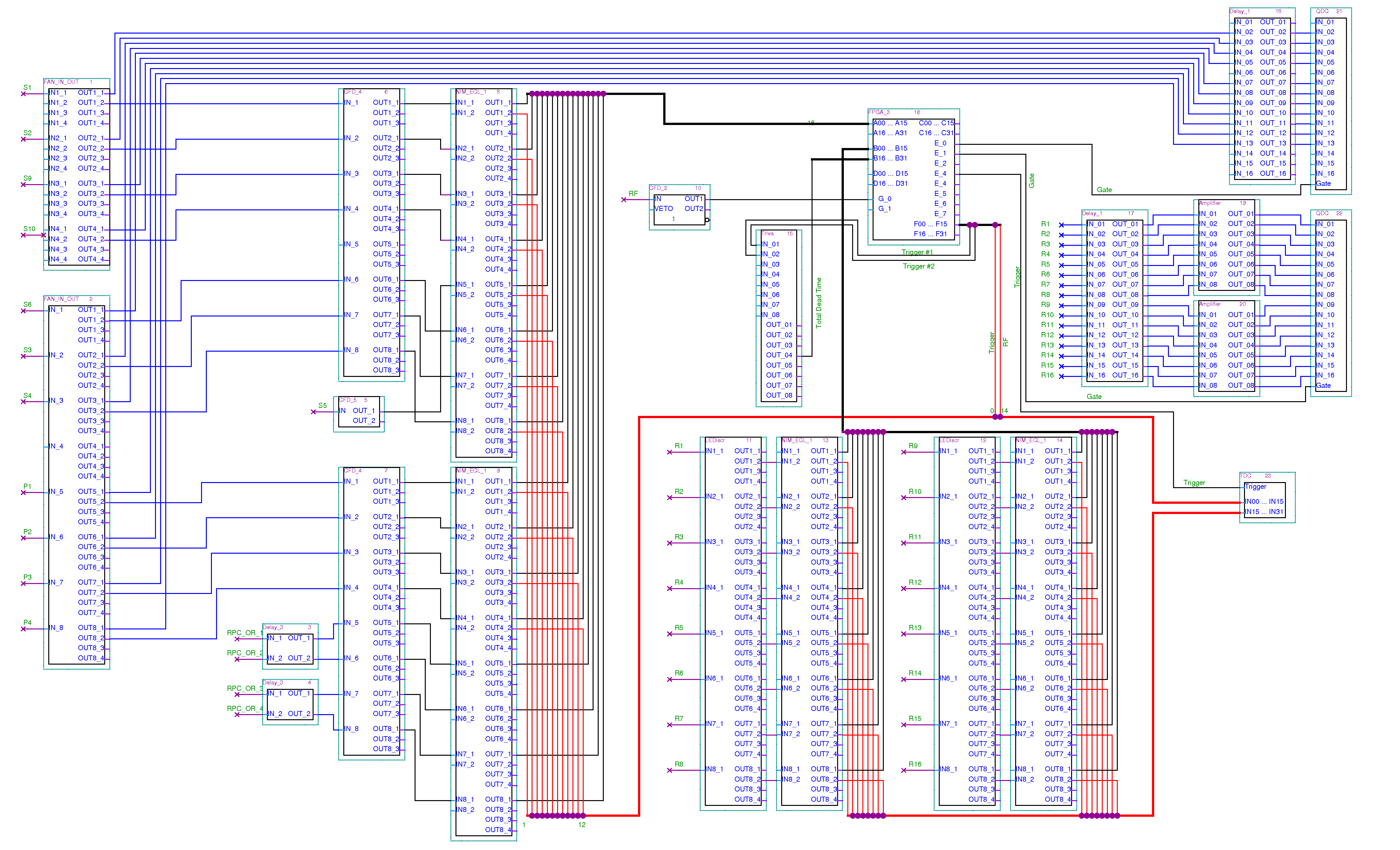
Electronics for NeuLAND MRPC Experiments (FPGA version)
| module | crate | base address | number | channels / units | application | scheme id. |
| RIO 5 | VME | VME master | 1 | - | data acquisition and data transfer | - |
| TRIVA | VME | 0x02000000 | 1 | - | trigger module | 15 |
| CAEN V1495 General Purpose VME Board | VME | 0x05120000 | 1 | 128 inputs 64 outputs |
trigger logic QDC gate generation Scaler |
16 |
| CAEN V1290 TDC | VME | 0x04000000 | 1 | 32 | timing measurement | 23 |
| CAEN V965 QDC | VME | 0x03400000 | 2 | 16 | charge measurement | 21, 22 |
| CAEN V538A NIM/ECL conv. | VME | - | 2 | 8 | fast NIM to ECLconversion of scintillator signals | 8, 9 |
| CAEN V538A NIM/ECL conv. | VME | - | 2 | 8 | fast NIM to ECLconversion of RPC time signals | 13, 14 |
| Phillips Scientific 710 | NIM | - | 2 | 8 | discrimination (leading edge) RPC time signals | 11, 12 |
| Ortec CF8000 | NIM | - | 2 | 8 | discrimination (constant fraction) scintillator signals | 6, 7 |
| CFD (HZDR home made) | NIM | - | 1 | 5 | discrimination (constant fraction) RF signal | 10 |
| CFD | - | - | 1 | 1 | discrimination (constant fraction) scintillator signal S5 | 5 |
| LeCroy 428F | NIM | - | 1 | 4 | linear FAN IN/OUT for scintillator signals | 1 |
| Phillips Scientific 748 | NIM | - | 1 | 8 | linear FAN IN/OUT for scintillator signals | 2 |
| Philips Scientific 775 | NIM | - | 1 | 8 | fast amplifier for RPC signals | 19, 20 |
| Delay | NIM | - | 6 | 2 x 64ns | delay of scintillator signals and RPC ORs | 3, 4, 18 |
| Delay (HZDR home made) | NIM | - | 2 | 8 x 140ns | delay of RPC signals for QDC inputs | 17 |
TDC and QDC channels for NeuLAND MRPC Experiments
| TDC channel | geo address : channel lmd file |
Signal | QDC channel | geo address : channel lmd file |
Signal |
| 0 | 5 : 0 | Trigger | 0 | 7 : 0 | - |
| 1 | 5 : 1 | S1 | 1 | 7 : 1 | S1 |
| 2 | 5 : 2 | S2 | 2 | 7 : 2 | S2 |
| 3 | 5 : 3 | S3 | 3 | 7 : 3 | S3 |
| 4 | 5 : 4 | S4 | 4 | 7 : 4 | S4 |
| 5 | 5 : 5 | S5 | 5 | 7 : 5 | - |
| 6 | 5 : 6 | S6 | 6 | 7 : 6 | S6 |
| 7 | 5 : 7 | S9 | 7 | 7 : 7 | S9 |
| 8 | 5 : 8 | S10 | 8 | 7 : 8 | S10 |
| 9 | 5 : 9 | P1 (ROLU R) | 9 | 7 : 9 | P1 (ROLU R) |
| 10 | 5 : 10 | P2 (ROLU O) | 10 | 7 : 10 | P2 (ROLU O) |
| 11 | 5 : 11 | P3 (ROLU L) | 11 | 7 : 11 | P3 (ROLU L) |
| 12 | 5 : 12 | P4 (ROLU U) | 12 | 7 : 12 | P4 (ROLU U) |
| 13 | 5 : 13 | - | 13 | 7 : 13 | - |
| 14 | 5 : 14 | RF | 14 | 7 : 14 | - |
| 15 | 5 : 15 | - | 15 | 7 : 15 | - |
| 16 | 5 : 16 | R1 | 16 | 8 : 0 | R1 |
| up to | up to | up to | up to | up to | up to |
| 31 | 5 : 31 | R16 | 31 | 8 : 15 | R16 |
Function of V1495 General Purpose VME Board (FPGA)
- Trigger Logic
We use two independent triggers for the NeuLAND MRPC data acquisition. Trigger number 1 is generated out of the coincidence signal of the scintillators and the RF signal. Trigger number 2 is generated out of the LNE (Load Next Event) signal from the V1495 scaler part. The LNE signal occurs when the scaler has reached the user defined prescale value and copies the current scaler values into the output registers. There we need the scaler values for efficiency calculation and beam adjustment we have to make sure that every trigger generated by the scaler passes. Therefore we have create an "keep alive circuit" which delays the trigger number 2 as long as necessary.
Refer the manual to see how to set the coincidence conditions. - QDC gate generation
The V1495 generates the gates for the QDC using the internal delay lines. The gates are opened with the leading edge of the trigger and the gate widths are independently adjustable within 1 ns steps according to the formula:
tgate = 25 ns + x · 1 ns x = [1 ... 255]
Refer the manual to see how to set the gate widths. - Scaler
The V1495 operates as 24 bit scaler with 68 channels. The FPGA counts the leading edges of the incoming signals. The required coincidences are produced inside the FPGA. Reaching the scaling time the FPGA copies the scaler values into the output register and clear all scaler channels.
There are three additional scaler channels with 64 bit depth for real time, dead time and live time measurement. Those scalers counting the internal 40 MHz clock singals as long as the scaler is active, active and busy or active and not busy, respectively.
Refer the manual to see how to set the scaling time.
Scaler usage for NeuLAND MRPC Experiments
(stand: 25.01.2010)
| channel scaler |
geo address : channel lmd file |
name | channel scaler |
geo address : channel lmd file |
name | channel scaler |
geo address : channel lmd file |
name |
| 1 | 13 : 0 | S1 | 25 | 14 : 0 | R15 | 49 | 15 : 0 | R3R4 |
| 2 | 13 : 1 | S2 | 26 | 14 : 1 | R16 | 50 | 15 : 1 | R5R6 |
| 3 | 13 : 2 | S3 | 27 | 14 : 2 | ROLU right | 51 | 15 : 2 | R7R8 |
| 4 | 13 : 3 | S4 | 28 | 14 : 3 | ROLU top | 52 | 15 : 3 | R9R10 |
| 5 | 13 : 4 | S5 | 29 | 14 : 4 | ROLU left | 53 | 15 : 4 | R11R12 |
| 6 | 13 : 5 | S6 | 30 | 14 : 5 | ROLU bottom | 54 | 15 : 5 | R13R14 |
| 7 | 13 : 6 | S7 | 31 | 14 : 6 | ROLU OR | 55 | 15 : 6 | R15R16 |
| 8 | 13 : 7 | S8 | 32 | 14 : 7 | ROLU OR & Trigger | 56 | 15 : 7 | R1R2R3R4 |
| 9 | 13 : 8 | S9 | 33 | 14 : 8 | S1S2 | 57 | 15 : 8 | R3R4R5R6 |
| 10 | 13 : 9 | S10 | 34 | 14 : 9 | S3S4 | 58 | 15 : 9 | R5R6R7R8 |
| 11 | 13 : 10 | R1 | 35 | 14 : 10 | S9S10 | 59 | 15 : 10 | R7R8R9R10 |
| 12 | 13 : 11 | R2 | 36 | 14 : 11 | S1S2S3S4 | 60 | 15 : 11 | R9R10R11R12 |
| 13 | 13 : 12 | R3 | 37 | 14 : 12 | S1S2S9S10 | 61 | 15 : 12 | R11R12R13R14 |
| 14 | 13 : 13 | R4 | 38 | 14 : 13 | Trigger | 62 | 15 : 13 | R13R14R15R16 |
| 15 | 13 : 14 | R5 | 39 | 14 : 14 | Trigger_DAQ | 63 | 15 : 14 | R1R2R3R4R5R6 |
| 16 | 13 : 15 | R6 | 40 | 14 : 15 | Trigger & RPC OR1 | 64 | 15 : 15 | R3R4R5R6R7R8 |
| 17 | 13 : 16 | R7 | 41 | 14 : 16 | Trigger & RPC OR2 | 65 | 15 : 16 | R5R6R7R8R9R10 |
| 18 | 13 : 17 | R8 | 42 | 14 : 17 | Trigger & RPC OR3 | 66 | 15 : 17 | R7R8R9R10R11R12 |
| 19 | 13 : 18 | R9 | 43 | 14 : 18 | Trigger & RPC OR4 | 67 | 15 : 18 | R9R10R11R12R13R14 |
| 20 | 13 : 19 | R10 | 44 | 14 : 19 | RPC OR1 | 68 | 15 : 19 | R11R12R13R14R15R16 |
| 21 | 13 : 20 | R11 | 45 | 14 : 20 | RPC OR2 | 69 | 15 : 20 | ROLU top right |
| 22 | 13 : 21 | R12 | 46 | 14 : 21 | RPC OR3 | 70 | 15 : 21 | ROLU top left |
| 23 | 13 : 22 | R13 | 47 | 14 : 22 | RPC OR4 | 71 | 15 : 22 | ROLU bottom left |
| 24 | 13 : 23 | R14 | 48 | 14 : 23 | R1R2 | 72 | 15 : 23 | ROLU bottom right |
| 73 | 15 : 24 | Trigger (MP) | ||||||
| 74 | 15 : 25 | Trigger (BW) | ||||||
| 75 | 15 : 26 | Trigger_DAQ (MP) | ||||||
| - | 16 : 0 | real time low | - | 16 : 3 | live time low | - | 16 : 6 | dead time low |
| - | 16 : 1 | real time mid | - | 16 : 4 | live time mid | - | 16 : 7 | dead time mid |
| - | 16 : 2 | real time high | - | 16 : 5 | live time high | - | 16 : 8 | dead time high |
| - | 16 : 9 | real time (MP) low | - | 16 : 12 | dead time (MP) low | |||
| - | 16 : 10 | real time (MP) mid | - | 16 : 13 | dead time (MP) mid | |||
| - | 16 : 11 | real time (MP) high | - | 16 : 14 | dead time (MP) high | |||
Timestamp (FPGA) for NeuLAND MRPC Experiments
(stand: 25.01.2010)
| geo address : channel lmd file |
name | geo address : channel lmd file |
name | geo address : channel lmd file |
name | geo address : channel lmd file |
name |
| 21 : 0 | Timestamp 1 low | 21 : 2 | Timestamp 2 low | 21 : 4 | Timestamp 3 low | 21 : 6 | Timestamp 4 low |
| 21 : 1 | Timestamp 1 high | 21 : 3 | Timestamp 2 high | 21 : 5 | Timestamp 3 high | 21 : 7 | Timestamp 4 high |
| 21 : 8 | block window low | ||||||
| 21 : 9 | block window high |
| timestamp | signal | resolution | clock | information | reset |
| 1 | Trigger_DAQ leading edge |
25 ns | internal FPGA clock | bit (47 downto 0) -> timestamp | with start of acquisition |
| 2 | Trigger_DAQ leading edge |
10 ns | external clock | bit (47 downto 0) -> timestamp | with start of acquisition |
| 3 | Trigger_DAQ leading edge |
25 ns | internal FPGA clock | bit (47 downto 35) -> no information bit 34 -> block window flag bit 33 -> macro pulse flag bit 32 -> macro pulse input flag (only for debugging) bit (32 downto 0) -> timestamp |
with leading edge of macro pulse |
| 4 | macro pulse leading edge |
25 ns | internal FPGA clock | bit (47 downto 0) -> timestamp | with start of acquisition |
High Voltage
(stand: 23.03.2010)
| Name | Channel | Voltage | cable |
| S1 | 0 | -1850V | HV1 |
| S2 | 1 | -1800V | HV2 |
| S3 | 2 | -1850V | HV3 |
| S4 | 3 | -1800V | HV4 |
| S5 | 12 | -700V | HV5 |
| S6 | 13 | -1700V | HV13 |
| S9 | 11 | -1600V | HV9 |
| S10 | 10 | -1600V | HV10 |
| P1 | 4 | -1650V | HV7 |
| P2 | 5 | -1650V | HV8 |
| P3 | 6 | -1580V | HV11 |
| P4 | 7 | -1600V | HV12 |

