| Machine |
Details |
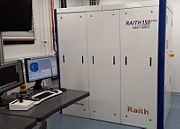 Electron beam writer
RAITH 150 TWO
|
- Manufacturer: RAITH GmbH
- Applications:
- Electron source:
- 30 kV Schottky thermal field electron emitter ZrO/W
- Sample size: ≤ 4 inch wafer
- Smallest feature size: sub 8 nm
- Sample stage with laser interferrometer
- Height sensing and FBMS mode available
- GDSII editor for generation of complex structure design on several layers with individual dose factor assignment for single structrure elements
- NanoPECSTM software suite for the correction of proximitty effects
Responsible: Dr. Y. Georgiev, Y.Georgiev@hzdr.de, 0351 / 260 - 2321
|
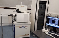 Electron beam writer
RAITH eLiNE plus
|
- Manufacturer: RAITH GmbH
- Applications:
- Nanolithography
- Imaging
- Nanoengineering
- Electron source:
- 30 kV Schottky thermal field electron emitter ZrO/W
- Sample size: ≤ 3 inch wafer
- Smallest feature size: sub 5 nm
- Sample stage with laser interferrometer
- 4 integrated nanomanipulators for e.g. nanoprobing
- Height sensing mode available
- GDSII editor for generation of complex structure design on several layers with individual dose factor assignment for single structrure elements
- NanoPECSTM software suite for the correction of proximitty effects
Responsible: Dr. Y. Georgiev, Y.Georgiev@hzdr.de, 0351 / 260 - 2321
|
Deposition and annealing |
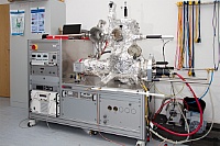 UHV evaporation tool UHV evaporation tool
BETty
|
- Manufacturer: BESTEC GmbH
- Base pressure <10-9 mbar
- E-gun evaporator (7 pockets)
- Thermal evaporator (Al)
- Temperature range 130 K – 600 K
- Tilt range ±45°
- Sputter gun (sample cleaning)
- Application: Metal film deposition
Responsible: Dr. Y. Georgiev, Y.Georgiev@hzdr.de, 0351 / 260 - 2321
|
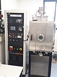 Evaporation tool Evaporation tool
LAB500
|
- Manufacturer: Leybold Optics
- Base pressure <10-7 mbar
- Substrate diameter: max. 100 mm
- Substrate thickness: max. 25 mm
- E-gun evaporator (4 pockets)
- Thermal evaporator (2 sources)
- Application: Metal film deposition
Responsible: Dr. Y. Georgiev, Y.Georgiev@hzdr.de, 0351 / 260 - 2321
|
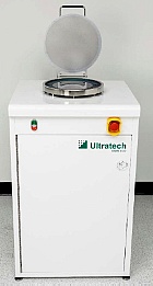 Atomic layer deposition
|
- Manufacturer: Ultratech/CambridgeNanotechALD
- Substrate size: ≤ 4 inch wafer
- Temperature: 80 - 350°C
- Materials:
- Al2O3
- HfO2
- SiO2
- mixed layers (on request)
Responsible: Dr. L. Rebohle, l.rebohle@hzdr.de, 0351 / 260 - 3368, Dr. Y. Georgiev, Y.Georgiev@hzdr.de, 0351 / 260 - 2321
|
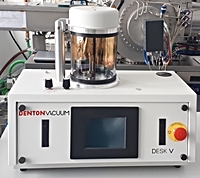 Sputter Coater
Desk V
|
|
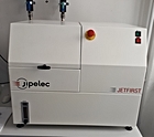 Rapid thermal annealing
JetFirst 100
|
- Manufacturer: Jipelec
- Substrate size: ≤. 4 inch wafer
- Temperature: ≤ 1300°C
- Gases: Ar, N2
Responsible: Dr. S. Winnerl, s.winnerl@hzdr.de, 0351 / 260 - 3522, Dr. Y. Georgiev, Y.Georgiev@hzdr.de, 0351 / 260 - 2321
|
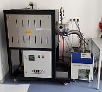 High vacuum oven
XERION X-TUBE
|
- Manufacturer: XERION ADVANCED HEATING® Ofentechnik GmbH
- Sample size: ≤ 4 inch wafer
- Temperature range: ≤ 800°C
- Pressure: down to 4*10-7 mbar
- Gas: N2
- Ramp rates for heating up and cooling down
Responsible: Dr. Y. Georgiev, Y.Georgiev@hzdr.de, 0351 / 260 - 2321
|
Etching and cleaning |
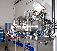 Reactive ion beam etcher
IonSys 500
|
- Manufacturer: ROTH & RAU AG
- Applications:
- Non-selective etching by sputtering with Ar gas
- Anisotropic etching of:
- Metals
- Magnetic stacks
- SiO2
- Sample size: ≤ 6 inch wafer
- Ar source
- Etch gas: CF4
- Helium backside cooling
- Sample tilting: ≤ 90°
- Sample rotation: ≤ 10 rpm
- Secondary Ion Mass Spectrometer (SIMS) manufactured by Hiden Analytical, UK for end point detection
Responsible: Dr. Y. Georgiev, Y.Georgiev@hzdr.de, 0351 / 260 - 2321
|
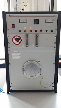 Plasma cleaner
PICO
|
- Manufacturer: DIENER ELECTRONIC GmbH + Co. KG
- Applications:
- Activating of semiconductors
- Cleaning of semiconductors
- Etching of semiconductors
- Plasmapolymerisation
- Sample size: ≤ 4 inch wafer
- Gases: O2, Ar
, N2
- Frequency: 2,45 GHz
- Power: 0 - 300W
- Faraday box for electrical sensitive components
- Piranisensor is measuring the pressure below 10 mbar
- Power display of the generator
- Timer for setting the process time up to 999,9 min
Responsible: Dr. Y. Georgiev, Y.Georgiev@hzdr.de, 0351 / 260 - 2321
|
Electrical characterisation |
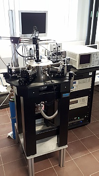 Cryogenic probe station
CPX-VF
![]()
|
- Manufacturer: LAKESHORE
- Applications:
- C-V measurements
- I-V measurements
- 4-Probe measurements
- Hall measurements
- Microwave measurements
- Electro-optical measurements
- all measurements can be combined with out-of-plane vertical field superconducting magnetic measurements
- Sample size: ≤ 2 inch wafer
- Magnetic field: ∓ 2,5 T
- Orientation of the magnetic field: vertical out-of-plane
- Temperature range: 4.5 K – 400 K
- Available sample holder:
- grounded sample holder
- coaxial sample holder
- tiltable sample holder
- Orientation of the magnetic field can be changed to in-plane
- Measuring instruments:
- AGILENT 4156C Precision Semiconductor Parameter Analyzer
- LakeShore 625 Superconductiong magnet power supply
- LakeShore 340 Temperature controller
- LakeShore 332 Temperature controller
- Incoupling of a laser signal (λ = 473nm / 785nm) possible
- Multiple radiation shields for best low temperature performance
- Minimize sample condensation during cool-down
- True 90° probing
Responsible: Dr. A. Erbe, a.erbe@hzdr.de, 0351 / 260 - 2366>
|
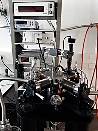 Cryogenic probe station Cryogenic probe station
TTP-4A
![]()
|
- Manufacturer: LAKESHORE
- Applications:
- C-V measurements
- I-V measurements
- Microwave measurements
- Electro-optical measurements
- Sample size: ≤ 2 inch wafer
- Temperature range: 4.5 K – 400 K
- Available sample holder:
- grounded sample holder
- coaxial sample holder
- Measuring instruments:
- AGILENT 4156C Precision Semiconductor Parameter Analyzer
- AGILENT 34410A Digital Multimeter
- KEITHLEY 2400 Source Meter
- LakeShore 332 Temperature controller
- Incoupling of a laser signal (λ = 473nm / 785nm) possible
- Radiation shield for best low temperature performance
- Minimize sample condensation during cool-down
- True 90° probing
Responsible: Dr. A. Erbe, a.erbe@hzdr.de, 0351 / 260 - 2366>
|
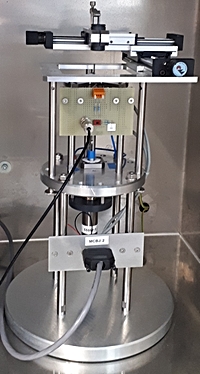 Mechanically controlled Mechanically controlled
break junction setup
![]()
|
- Applications:
- Electrical characterization of molecular structures
- at room temperature
- in liquid environment
- Currently investigated molecules:
- Selenium metal complexes
- Polythiophenes
- Bucky-bowl structures (e.g. Corannulene)
- Currently investigated solvents:
- Current measurement in the range of Femto-Ampere due to electrical and magnetic shielding technology
- 4 setups
-
Responsible: Dr. A. Erbe, a.erbe@hzdr.de, 0351 / 260 - 2366
|
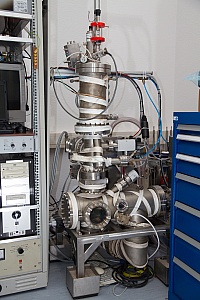 Cryogenic UHV Cryogenic UHV
break junction setup
|
- Applications:
- I-V measurements
- Ploting histograms of the conductance
- Inelastic electron tunneling spectroscopy (IETS)
- Point-contact spectroscopy (PCS)
- Temperature range: 5 K – 300 K
- Pressure (at low temperatures): 5*10-5 mbar
- In situ deposition of molecules into the break junctions
- Via thermal evaporation of e.g. C60
- Depostion rate: 0,2 Å/s - 0,6 Å/s
- Thicknesses of ¼ up to 1 monolayer
- Measuring instruments:
- KEITHLEY 2400 Source Meter
- KEITHLEY 6430 Sub Femtoamp Remote Source Meter
- LakeShore 331 Temperature controller
- YOKOGAWA 7651 Programmable DC Source
Responsible: Dr. A. Erbe, a.erbe@hzdr.de, 0351 / 260 - 2366
|
Optical characterisation |
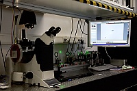 Optical tweezers
|
- tool for ...
- Application: ...
Responsible: ...
|
Sample preparation and lab equipment |
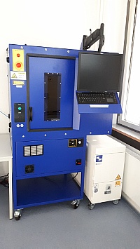 Laser cutter
skylaser MARK 20
|
- Manufacturer: PFEIFER technology & innovation
- Applications:
- Surface graving and labeling
- Cutting of wood, plastics, (to some extend) Silicon
- Sample size: up to 110 x 110 cm²
- Alignment accuracy: ~ 0,1mm
- Laser power: 20 W
- Laser source: Ytterbium pulsed fiber laser
- Wavelength: 1064nm
- Speed: max. 10.000 mm/s
- Frequency: 20 - 80kHz
Responsible: Dr. Y. Georgiev, Y.Georgiev@hzdr.de, 0351 / 260 - 2321
|
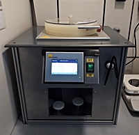 Spin Coater
LabSpin 6
|
- Manufacturer: SÜSS MicroTec
- Applications:
- Spin coat resists for electron beam lithography
- Sample size: ≤ 4 inch wafer
- Rotation speed: ≤ 8000 rpm
Responsible: Dr. Y. Georgiev, Y.Georgiev@hzdr.de, 0351 / 260 - 2321
|
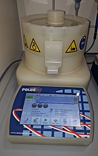 Spin Coater
POLOS Spin150i
|
- Manufacturer: SPS Europe
- Applications:
- Sample size: ≤ 4 inch wafer
- Rotation speed: ≤ 12.000 rpm
Responsible: Dr. Y. Georgiev, Y.Georgiev@hzdr.de, 0351 / 260 - 2321
|
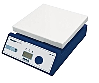 Hotplate
HP-20D
|
- Manufacturer: witeg Labortechnik GmbH
- Applications:
- Pre/Post bake of EBL resist
- Sample cleaning
- Lift off processes
- Sample size: 180 mm x 180 mm
- Temperature: ≤ 380°C
Responsible: Dr. Y. Georgiev, Y.Georgiev@hzdr.de, 0351 / 260 - 2321
|
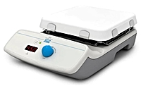 Hotplate
Velp Scientifica
|
- Manufacturer: VelpScientifica
- Applications:
- Pre/Post bake of EBL resist
- Sample cleaning
- Lift off processes
- Sample size: 180 mm x 180 mm
- Temperature: ≤ 550°C
Responsible: Dr. Y. Georgiev, Y.Georgiev@hzdr.de, 0351 / 260 - 2321
|
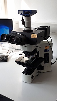 Optical microscope
OPLYMPUS BX51
|
- Manufacturer: OLYMPUS GmbH
- Magnifications: 5x, 10x, 20x, 50x, 100x, 250x
- Dark field and bright field mode
- Transmitted light and reflected light mode
- Taking images with the installed camera (Carl Zeiss Axio Cam MRc)
Responsible: Dr. Y. Georgiev, Y.Georgiev@hzdr.de, 0351 / 260 - 2321
|
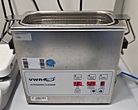 Ultrasonic bath
USC 300D
|
- Manufacturer: VWR
- Ultrasonic frequency: 45 kHz
- Ultrasound power: 32 - 80 W (9 power levels)
- Temperatur: ≤ 80°C
- Time: ≤ 99 min
- Degas function
Responsible: Dr. Y. Georgiev, Y.Georgiev@hzdr.de, 0351 / 260 - 2321
|
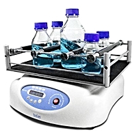 Multi-functional orbital shaker
PSU-20i
|
- Manufacturer: bioSan
- Orbital rotation:
- Speed control range: 20 -250 rpm
- Increment: 5 rpm
- Time setting range: ≤ 250 s per cycle
- Reciprocal motion:
- Amplitude range: 0 - 360°
- Increment: 30°
- Time setting range: ≤ 250 s per cycle
- Vibro motion:
- Amplitude range: 0 - 5°
- Increment: 1°
- Time setting range: ≤ 5 s per cycle
- Load: max 8 kg (below 150 rpm)
Responsible: Dr. Y. Georgiev, Y.Georgiev@hzdr.de, 0351 / 260 - 2321
|
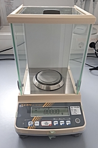 High precision scale
ABJ120
|
- Manufacturer: Kern
- Max. weight: 120 g
- Min. weight: 10 mg
- Readability: 0,1 mg
Responsible: Dr. Y. Georgiev, Y.Georgiev@hzdr.de, 0351 / 260 - 2321
|
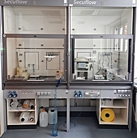 Fume hood
Secuflow
|
- Manufacturer: Waldner
- Volume flow: at least 330 m³/h
Responsible: Dr. Y. Georgiev, Y.Georgiev@hzdr.de, 0351 / 260 - 2321
|
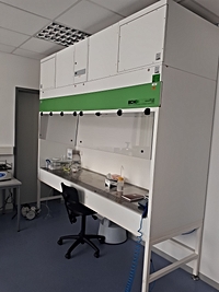 Laminar flowbox
|
- Manufacturer: BDK Luft- und Reinraumtechnik GmbH
- Filter class: H14
Responsible: Dr. Y. Georgiev, Y.Georgiev@hzdr.de, 0351 / 260 - 2321
|
Planned experimental setups |
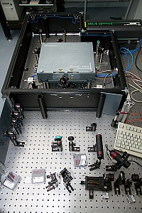 Asynchronous Optical Sampling (ASOPS)
|
- Application
- Optical characterization of nanomechanical resonators
Responsible: Dr. A. Erbe, a.erbe@hzdr.de, 0351 / 260 - 2366
|


