The RP/2 Effect
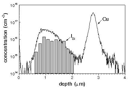
By high-energy ion implantation a damage is created in the whole depth range from the wafer surface to ~ RP + D RP (mean projected range: RP). Despite of damage annealing at T= 900oC strong impurity gettering has been detected at depths between the surface and RP [1-4] This is called the RP/2 effect. The size of the defects responsible for the gettering at RP/2 is below the resolution limit of transmission electron microscopy (TEM). They are very small defect clusters.Recently we have reported [3] that defects at RP/2
can be observed by TEM. TEM observations for a specific ion milling procedure
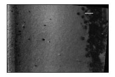
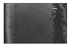
reveal the presence of interstitial-type loops (Fig. 1).
 |
a) | |
|
|
 |
b) |
|
|
 |
c) |
|
|
 |
d) |
|
|
 |
e) |
Fig. 1
(a) SIMS Cu depth profile for FZ-Si after FA at 850°C/1h. correlated
with the concentration of self-interstitials bound in loops (bars);
(b, c, d, e) XTEM bright field micrographs. The sample is the same
as in (a).The incidence angle for milling is 13° (b), 15° (c),
17° (d) and 4° (e). The bar in the micrographs corresponds to 200
nm.
These loops appear by injection of self-interstitial atoms during ion milling process (Fig. 2).

Fig. 2
A scheme of a cross-sectional sample, milling incidence angle.
Results of our study:
The interstitials caused by the ion milling procedure modify significantly
the defect structure of previously MeV self-ion-implanted and annealed
Si samples.
The interstitial loops appear only in the RP/2 region. The
presence of copper in the sample does not play role in the formation
of the defects during milling [3].
The real gettering centres for Cu atoms at RP/2 are suggested
[4] be self-interstitial clusters, too small to be visible by XTEM.
References
[1] R. Kögler, D. Panknin, W. Skorupa, P.
Werner, and A. Danilin
Proc. of the XI Int. Conf. Ion Implantation and Technology
96, IEEE Publ. 96TH8182, Piscataway, NJ 08854-4150.
[2] R.Kögler, M.Posselt, R.A. Yankov, J.R. Kaschny, P. Werner,
A.B. Danilin, and W. Skorupa
Mat. Res. Symp. Proc. Vol. 469, 463 (1997)
[3] A. Peeva, R.Kögler, G. Brauer, W. Skorupa, and P.Werner
1st ENDEASD Workshop Proc. p. 269, Santorini April
1999, Greece
[4] R.Kögler, A. Peeva, W. Anwand, G. Bauer, P. Werner, W. Skorupa,
and U. Gösele
Appl. Phys. Lett. 75, 1279 (1999)

